


Description
Silicon Carbide (SiC) MOSFET use a completely new technology that provide superior switching performance and higher reliability compared to Silicon. In addition, the low ON resistance and compact chip size ensure low capacitance and gate charge. Consequently, system benefits include highest efficiency, faster operating frequency, increased power density, reduced EMI, and reduced system size.
● High Blocking Voltage with Low RDS(on)
● Simple to drive with Standard GateDrive
● 100% avalanche tested
● Maximum junction temperature of150°C
● ROHSCompliant
●EVCharging
● DC‐ACInverters
● High Voltage DC/DCConverters
● Switch Mode PowerSupplies
● Power Factor CorrectionModules
● MotorDrives
Ordering Information
Absolute Maximum Ratings(Tc=25℃)
|
Symbol |
Parameter |
Value |
Unit |
|
VDS |
Drain-Source Voltage |
1200 |
V |
|
ID |
Drain Current(continuous)at Tc=25℃ |
100 |
A |
|
ID |
Drain Current(continuous)at Tc=100℃ |
68 |
A |
|
IDM |
Drain Current (pulsed) |
200 |
A |
|
VGS |
Gate-Source Voltage |
-10/+20 |
V |
|
PD |
Power Dissipation TC= 25°C |
420 |
W |
|
TJ,Tstg |
Junction and Storage Temperature Range |
-55 to +150 |
℃ |
|
|
Symbol |
Parameter |
Test Conditions |
Min. |
Typ. |
Max. |
Unit |
|
BVDS |
Drain-source Breakdown Voltage |
ID=250uA,VGS=0V |
1200 |
|
|
V |
|
IDSS |
Zero Gate Voltage Drain Current |
VDS=1200V, VGS=0V, TJ=25°C |
|
|
100 |
uA |
|
IGSS |
Gate-body Leakage Current |
VDS=0V ; VGS=10 to 20V |
|
|
250 |
nA |
|
VGS(th) |
Gate Threshold Voltage |
VDS= VGS,ID=15mA |
2 |
|
4 |
V |
|
RDS(on) |
Static Drain-source On Resistance |
VGS=18V, ID=50A |
|
20 |
30 |
mΩ |
|
RG |
Gate Resistance |
VGS=0V,f=1MHz |
|
3 |
|
W |
Typical Performance‐Dynamic
|
Ciss |
Input Capacitance |
VDS=800V,f=1000KHZ,VGS=0V |
|
4890 |
|
pF |
|
Coss |
Output Capacitance |
|
130 |
|
pF |
|
|
Crss |
Reverse Transfer Capacitance |
|
22 |
|
pF |
|
|
Qg |
Total Gate Charge |
VDS=800V,ID=50A,VGS=0~20V |
|
166 |
|
nC |
|
Qgs |
Gate-source Charge |
|
58 |
|
nC |
|
|
Qgd |
Gate-Drain Charge |
|
48 |
|
nC |
|
|
td(on) |
Turn-on Delay Time |
VDD=800V,ID=50A,VGS=-0V~20V,RG=0Ω, |
|
150 |
|
ns |
|
tr |
Rise Time |
|
30 |
|
ns |
|
|
td(off) |
Turn-off Delay Time |
|
80 |
|
ns |
|
|
tf |
Fall Time |
|
28 |
|
ns |
Typical Performance‐Reverse Diode
|
Symbol |
Parameter |
Test Conditions |
Min. |
Typ. |
Max. |
Unit |
|
VFSD |
Forward Voltage |
VGS=0V,IF=30A,TJ=25°C |
2 |
|
5 |
V |
|
VGS=0V,IF=30A,TJ=150°C |
2 |
|
5 |
V |
||
|
trr |
Reverse Recovery Time |
VGS=0 V, IF=30 A, VR=800 V, di/dt=100 A/μs |
|
90 |
|
ns |
|
Qrr |
Reverse Recovery Charge |
|
880 |
|
nC |
|
|
Irrm |
Peak Reverse Recovery Current |
|
21 |
|
A |
Thermal Characteristics
|
Symbol |
Parameter |
Value. |
Unit |
|
RqJC |
Thermal Resistance, Junction-to-Case |
0.3 |
°C/W |
|
RqJA |
Thermal Resistance, Junction-to-Case |
40 |
°C/W |
The values are based on the junction-to case thermal impedance which is measured with the device mounted to a large heat sink assuming maximum junction temperature of Tj(max)=150℃
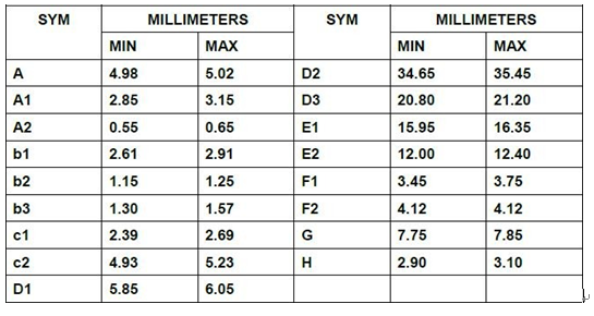
Dimensions(UNIT:mm)